Hybrid Microwave Systems

Hybrid microwave systems are the ones which are capable of transmitting TDM  data and FDM voice signals simultaneously.To be practical and sound economical it is better to convert the exiting FDM system into a hybrid one than to install a brand new digital system for some of the application.Hybrid  systems provide efficient means to transmit data at a rate of 1.544 Mb/sec,in addition to the FDM or the video message,on conventional,analog,FM microwave,cable,optical fiber systems and satellite systems.These systems can be modified to provide higher data rates too.
Fig. shown the transmitter block diagram of a typical 1.544 Mb/sec DUV(data under FDM voice).Here the data spectrum is kept within 0-470 kHz bandwidth which and the lowest FDM channel is at 564 kHz.Elastic store acts as a timing jitter removal circuit.The jitter free data signal is scrambled in a bit scrambler to suppress the high-power discrete spectral components.The advantage of scrambling is that the scrambled output data spectrum is continuous and has a predictable effect on the FDM  radio system data bandwidth which is compressed by the use of binary-to-7 level converter which is nothing but correlative coder. LPF  perform the function of suppressing the spectral power above 386 kHz (that can impair pilot control tone transmission or the quality of FDM channels) and final spectrum shaping   of the digital information. HPF in the FDM path assures that the bandwidth allocated for data transmission contains no analog signal.
The block diagram of 1.544 Mb/sec DUV receiver is shown in fig The digital  7-level information is low pass filtered and inputted to 7-level to binary converter circuit.Its output is descrambled and  converted into a 3-level bipolar signal useful for twisted.wire line transmission.Many operational FDM microwave systems use DUV system.
Digital Microwave system

These are also known as digital radio system,PCM radio system or digital line-of-sight microwave systems.A basic digital microwave system is shown in fig.Digital source block may have many PCM converted digitized voice channels,digital computer or other data channels.The transmitting block modulates the radio frequency carrier digitally by bit streams from digital source.After amplification,the modulated signal is radiated by a suitable antenna. Duplexer is employed to have the same antenna while transmitting or receiving.The receiver block demodulates the modulated signal and gives the digital message to the digital sink block which  in turn gives the original message.
For a digital microwave system two factors are important
(i)Source bit rate and
(ii)Digital signal code.
Transmission rate for low capacity microwave systems<=1Mb/sec.Transmission rate for high capacity microwave system >= 300 <=Mb/sec.
TDM-PCM channel banks are main sources of digital radio systems.Hence digital radio systems are also known as PCM radio systems.
The block diagram of a hypothetical one-way  PCM-radio path.According to CCIR definitions,hypothetical digital radio path contains 9 radio terminals connected by 9 higher order digital multiplex equipment  data rate of the system is 64 kb/sec at each end of the system and the system length is 2500 km. Digital input stream from the transmit section of TDM equipment is applied to the modulator of the   radio transmitter. 

Network Analyser

A network analyser is a network system that measures both amplitude and phase of a microwave signal over a wide frequency range in a reasonably small time.We may mention here that the slotted line could measure the amplitude and phase of a microwave signal only at a signal frequency.Moreover to make measurements at broad band frequencies using slotted line is both time consuming and costly in terms of manpower.
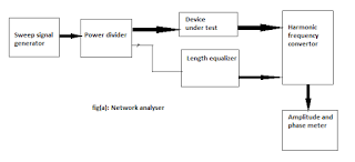
In a network analyser,the basic principle of measurement is to generate an accurate reference signal and compare this with respect to the test signal whose amplitude and phase are to be measured.A block schematic of a network analyser is shown in fig.

A sweep signal generator feeds a power divider or splitter that converts into two signals the test signal and the reference signal.The device under test (DUT) is fed with the test signal and length equalizer (phase equalising line) takes in the reference signal.These test and reference signals are than converted to standard IF frequency by a harmonic frequency converter.The output of the harmonic frequency converter is then used to determine the amplitude and phase of the test signal.
The harmonic frequency converter consists of a phase locked loop shown in fig 2 The local oscillator tracks the reference signal frequency making error possible swept frequency measurement.The double mixer arrangement  first converts the memory RF test signal to a first IF of 10 MHz and then a second IF of 278 kHz.

A network analyser is quite useful for measurement of both passive as well as active microwave components or network parameters.It is used for measurement of both  impedance (reflection) and gain (transmission) characteristics of microwave devices.It uses a stimulus response   method for testing over the frequency range of interest.As these parameters are a function of frequency with complex variables(having both magnitude and phase), a swept frequency measurement becomes imminent.

A network analyser can be scalar or vector.A scalar network analyser provides only magnitude characteristics of microwave devices as a function of frequency. A vector network analyser can of measurement in both these methods is the same in that they compare the incident or input power with the transmitter or reflected waves depending upon the parameter to be measured.The radio of the relevant signals is used to determine the scattering matrix of the DUT.

As explained earlier,we   have a signal source,power splitter,receiver/detector and a processor/display components.The DUT transmits or reflects the stimulating or incident signal from the signal sources which are used in the measurement of magnitude and phase of individual components of the test signal.The receiver and display could be a harmonic generator and the amplitude phase meter which have already been described.However in place of power splitter,we might have as well used a directional coupler or a higher impedance probe.

DIGITAL INSTRUMENTS

Digital instruments are becoming more and more popular because of their inherent advantages over analog instruments,such as,greater speed,increased accuracy,better resolution,reduction in operator errors and the ability to provide automatic measurement in system application.
Digital instruments use logic circuits and techniques for carrying out measurements of quantities.Any digital instrument may be viewed as an arrangement of logic gates that change states at very high speeds in the process of carrying out a measurement.
The major advantage of digital instruments is the readability of the measurement result because of the digital read-out.In analog instruments,the user performs the function of an analog-to-digital  converter(ADC).The user must read the analog scale properly,process some skill in interpolation,be able to use mirrored scales and in general,have a good eye.
The second major advantage of digital instruments over analog instruments is the accuracy.In general,digital instruments are more accurate than analog ones.For example,a low-cost digital multi meter.
Digital instruments provide better resolution than analog instruments. A typical values of resolution of a digital instrument may be one part in 1  µV can be read on the 1 -V input range.
The digital instruments also have greater speed.The maximum speed of reading and period of sampling is interrelated.
The digital voltmeters may have sampling rate from a few sample per second to 1000 samples per second.However,input capacitance and filter limits the sampling speed to 100 or below.Also,it is impossible to read out at high reading speed.
A digital instrument is quite different from an analog instrument with digital read-out.The circuit required for measurements  in a digital instrument is of  analog instrument with analog read-out,except that digital display is unambiguous and can be read more quickly.
Virtually all digital instruments provide a digital display of the measurand.A fixed number of pulses proportional to the measurand are entered in a digital counter and the counter actuates the digital display.So the counting circuits are vital parts of the digital instruments.
Digital instruments,particularly digital voltmeters of multi meters are employed for measurement of analog quantities.Conversion of an analog signal into an equivalent digital signal is,therefore,essential.Thus analog-to-digital converters (ADCs) are most important parts of digital instruments.

SILICON CONTROLLED RECTIFIER(SCR)

As the terminology indicates,the SCR is a controlled rectifier constructed of a silicon semiconductor material with a third terminal for control purposes.Silicon was chosen because of its high temperature and power capabilities.The basic operation of the SCR  is different from that of an ordinary two layer semiconductor diode in that a third terminal,called a gate,determines when the rectifier switches from the open-circuit to short-circuit state. It is not enough simply to forward bias the anode-to cathode region of the devices.In the conduction state the dynamic resistance of the SCR is typically 0.01 to 0.1Ω and reverse resistance is typically 100 kΩ or more.It is widely used as a switching device in power control applications.It can control loads y switching on and off up to many thousand times a second.It can switch on for a variable lengths of time duration,thereby delivering desired amount of power to the load.Thus,it possesses the advantage of a rheostat as well as a switch with none of their drawbacks.A schematic diagram and symbolic are shown fig.(a) and (b) respectively.fig(a) SCR is a three terminal four layer semiconductor devices,the layers being alternately of a P-type and N-type.The junctions are marked J1,J2 and J3(junction J1 and J3 operate in forward direction while middle junction j2 operates in the reverse direction) whereas the three terminals are anode (A),cathode (C) and gate (G) which is connected to the inner P-types layer.The function of the gate is to control the firing of SCR.In normal operating conditions,anode is positive with respect to cathode.

PULSE AND SQUARE-WAVE GENERATORS

These generators are often employed with an oscilloscope as the measuring devices.The waveforms displayed by the oscilloscope either at the output or at pertinent points in the system under test provide qualitative as well as quantitative information about the system or device under test.

These generators are designed for generating a periodic train of equal-amplitude pulses,as shown in fig.In pulse generators,the duration of the on time of a pulse may be independent of the time between pulses.However, if the pulse train has the property of being "on" 50 per cent ,the waveforms is called the square wave and the generators producing such waveform are called the square-wave generators.Thus square-wave generators can be considered to be a special class of pulse generators.
square-wave generators are used for investigating the low frequency characteristics of a system including testing of audio systems.Square waves are also preferred over short-duration pulses if the transient response of a system needs a comparatively high settling time.

Pulse generators are designed to generate pulses as close to ideal pulses as possible.High-quality pulses ensure that any distortion in the output pulse from a test circuit is owing to test circuit alone.The amplitude,pulse width,and period of the generated pulses are usually adjustable over various ranges.The duty cycle is also made adjustable;but in case the power contained by each  pulse is large,the maximum duty cycle must be kept small.As the maximum duty cycle of a pulse generator is reached,the waveform of the pulse become irregular or the pulse width no longer increases.
The output impedance of the pulse generator is an important consideration in fast pulse systems.This is so because the generator,which has a square impedance matched to the connecting cable,will absorb reflections resulting from impedance mismatches in the external circuitry.If it is not so,total absorption would not take place,a portion of the pulse would be re- reflected,and spurious pulses would appear to be generated from the pulse generator.

DC coupling of the output circuit is necessary when retention of the dc bias levels in the test circuit s desirable,inspite of variations in pulse width,pulse amplitude, or pulse repetition rate (PRR). 

WAVESHAPING

 waveshaping is a part of a signal processing where the signal waveform has to be properly shaped before amplification.It may be defined as a process of generating new waveforms by employing some network.In this process the output may vary in shape from input because of influence of the circuit elements on the signal.The influence of the circuit elements is determined by the ratio of output to input amplitude , and by the phase angle between the output and the input.Examples of waveshaping include alternation of a triangular wave into a square wave, and vice versa,alteration of a square wave into a series of narrow pulses,alternation of a square or triangular wave into a sinusoidal wave,and alternation of a sinusoidal wave into a square wave. Waveshaping  techniques are widely used in function generators,frequency synthesizers,and synchronization circuits that need different waveforms having precisely the same frequency.
Waveshaping may be of two types viz linear and non-linear waveshaping.
In linear waveshaping, signal  shape is altered by transmitting it through a linear network-a network consisting of linear element such as R,L and C.If a sinusoidal signal is applied to a linear network,then,in the steady state,the output signal will have the same waveshape as the input signal,though it may have amplitude and phase angle different from those of original signal.This feature of a sinusoidal signal to preserve its shape in all linear networks is unique.Thus R-C,R-L and R-L-C circuits are categorized as linear waveshaping circuits.such circuit are used to perform differentiation,integration and summation functions.
In nonlinear waveshaping,the shape of a signal is moderated by transmitting it through a nonlinear network.Nonlinear network consists of circuit elements having nonlinear transfer characteristics,such as diode,transistor,vacuum tube,in conjunction with other linear circuit elements.such circuits find application in amplitude limiting,clipping and clamping of signals.
In pulse circuitry there are many non-sinusoidal waveform such as step-pulse,square,ramp and exponential waveforms.
   

Switch mode Power supply(SMPS)

Switch mode power supply (SMPS) overcomes the limitations of regulated power supplies.Here in SMPS (or sometimes called switching regulator), the pass transistor is used as a controlled switch and is operated either in cutoff region or saturation region which makes the power transfer via the pass transistor in the form of discrete.
As in the case with other digital switching devices,this mode of operation results is very low power consumption.
SMPS are used in modern digital equipment such as telephone exchange,PCs,robotics etc.,battery powered equipment,video projectors,measuring instruments,space vehicles etc.Such system need very compact,light weight and highly energy efficient supplies. SMPS utilizes pulse width modulation to control  the average value of output voltage.The average value of the waveform depends on the area of waveform.If the TON time(or say,duty cycle (TON/TON+TOFF) is varied,the average value of voltage changes proportionately.
In the PWM switching at constant switching frequency,the switch control signal is generated by comparing Vcontrol and repetitive waveform .
SMPS or switching regulators can provide large load currents at low voltage precisely what is required in PCs (personal computers).
Switching regulators are available in three basic configuration viz. step-down,step-up and polarity inverting configurations.
Step-down version is shown in fig.The rectangular pulses on the base saturate and cut off the pass transistor during each cycle.This generates a rectangular voltage at the input to LC filter.This filter blocks the ac components and allows the dc components to pass to the output.Because of the on-off switching,the average value is always less than the input voltage.This is why the circuit is called the steep-down version.


EBERS-MOLL MODEL

Devices modelling aims at relating physical devices parameters to device terminal characteristics.Devices modeling is especially important for integrated circuits,since simple and accurate devices models are required to predict the performance of a circuit.Generally,by making a model more accurate,we make it more complex.Thus,there is a trade-off between accuracy and complexity.
Ebers-Moll model is a transistor model which describes the operating states of a transistor model which describes the operating states of a transistor.This model is useful to obtain information about the dc characteristics of a transistor.The transistor operates in active region when emitter junction is forward biased and collector junction is reverse biased.This model generalizes the behavior of a transistor by taking into account the inverted mode of operation of transistor.

BLOCK DIAGRAM OF A TYPICAL OPERATIONAL AMPLIFIER

An operational amplifier being a multistage amplifier,consists of some basic building blocks as shown in block diagram.
The block diagram of op-amp shown in fig.consists of a four stage direct-coupled amplifier in cascade.In summarized form,it can be explained as below.
The first stage is double-ended high-gain (60 dB) differential with a constant current source(in order to increase CMRR). In this stage high gain is desirable so that there would be a negligible effect on  the output of any shortcoming in the following stages. This is the reason why this stage is generally responsible for most of the gain of op-amp.Also this stage determines the input resistance of the op-amp.output of this stage is taken between collector of two emitter biased circuit so that output remains balanced and the dc voltage at output in quiescent condition maintains zero level.
The second stage,called the intermediate stage,is usually another differential amplifier,which is driven by the output of first stage, In most amplifier the intermediate stage is dual input,unbalanced (single-ended) output differential amplifier in order to increase the gain.The differential mode voltage gain of such an  amplifier is half of the gain of the dual-input,balanced output differential amplifier.In this amplifier output is  measured at the collector of only one of the two transistor w.r.t ground.In the quiescent condition some dc voltage exists at the output terminal and there is no other collector voltage at output to balance or nullify this output dc voltage.This is the reason why this type of amplifier is called unbalanced output type differential amplifier.This unbalanced dc voltage present at the output acts as an error voltage in the desired output signal.
The third stage,Known as level shifting   stage,is usually an emitter follower circuit in order to shift the dc level at the output of the intermediate stage downward to zero volt with respect to ground.It is noteworthy here that error signal is developed in the intermediate stage due to direct coupling and gets amplified in the succeeding stage.This increase in dc level tends to shift the operating point of the succeeding stages which also limits the output voltage swing or may distort the output signal.To overcome these problems, use of a level translator circuit becomes necessary to bring this dc level to zero volt.


TRANSISTORS

The transistor is a solid state device,whose operation depends upon the flow of electric charge carriers within the solid.Transistor is capable of amplification and in most respect it is analogous to a vacuum triode. The main difference between the two is that the transistor is a current controlled device whereas vacuum triode is a voltage controlled device.The transistor is only about 6 decade old, yet it has replaced vacuum tubes in almost all applications.The reasons are obviously its advantages over vacuum tubes such as compact size,light weight,rugged construction,more resistive to shocks and vibrations,instantaneous operation (no heating required),low operating voltage,high operating efficiency (no heat loss) and long life with essentially parature and frequency.However,transistor,in comparison to vacuum triodes, have  some drawbacks also such as loud hum noise,restricted operating temperature (up to 75°C) and operating frequency (up to a few MHz only).
It consists of a silicon or germanium (preferably silicon because of its smaller cutoff current  ICBO ,smaller variations in ICBO due to variations in temperature and higher operating temperature) crystal in which a layer of N-type material is sandwiched between two layers of P-type material,as shown in fig.Alternatively a transistor may consist of a layer of p-type material sandwiched between two layers of N-type material,as shown in fig.In the former case the transistor is referred to as a P-N-P transistor and in latter case,as an N-P-N transistor.Each type of transistor has two P-N junctions-one junction between the emitter and base,called the emitter-base junction or simply the emitter junction and the other junction between the base and collector,called the collector-base junction or simply the collector junction.Thus a transistor is like two P-N junction diodes connected back to back.The two junctions give rise to three regions provided with three terminals called the emitter,base and collector,as shown in fig.The emitter base,collector correspond in a general way to the the cathode, grid and plate or anode of vacuum triode.

DIODE DATA SHEET

For selection of a diode for a particular application,the data sheets provided by by the device manufacture must be consulted.
Most data sheets start off with the devices type number at the top of the sheet,a short descriptive title and a list of major application of the device.The information is usually followed by mechanical data in the form of illustration showing  the package shape and dimensions.The absolute maximum ratings of the diode at 25°C are listed next.These are maximum voltages,currents,temperature etc.,that the device can bear/carry without breaking down. It is very important,for the safe operation of the device,the maximum ratings given in the data sheets are never exceeded.For reliability the maximum ratings  should not even be approached.Also, the maximum rating must be adjusted downward for operation at temperature exceeding 25°C.Following the absolute maximum ratings,there is normally a complete list of electrical characteristics for the devices.Again,these are specified at 25°C, and allowances are necessary for variation of temperature.
some of the important parameters are considered below:
1.Peak reverse voltage or peak of voltage,VR or VRM.This is the absolute peak of voltage that must be applied in reverse across the diode.
2.steady-state forward current,I0 or IF.This is the maximum current that may be passed continuously through the diode.
3.peak forward surge current,IFM (surge).The surge current is very much higher than the normal maximum forward current.This rating defines the maximum value and the time interval for such surge in current level.It is a current that may flow briefly when a circuit is first switched on.
4.peak repetitive forward current is the maximum instantaneous value of repetitive forward current.This rating defines the maximum value and the time interval for such surge in current level.It is a current that level can be higher than the continuous level.
5.Average rectified current.A half-wave-rectifier signal has an average value defines y Iav=0.318 Ipeak .The average  current rating is lower than the continuous or peak repetitive forward currents because a half-wave current waveform will have instantaneous values much higher than the average value.
6.static maximum voltage drop,VF(max).This is the maximum forward voltage drop for a given forward current and device temperature.
7.Continuous power dissipation at 25°C,P.This is the maximum power that the device can safely dissipate on a continuous basis in free air. This rating must be downgraded for operation at higher temperature,and may be upgraded when the device is mounted on a heat sink.
8.Reverse recovery time,trr .This is the maximum time for the device to switch from on to off.

AVALANCHE PHOTODIODE

The avalanche photodiode is similar to the P-N or PIN photodiode except that it is operated at high reverse-bias voltages so that impact ionization occurs,EHPs are created in the space charge region by photon absorption.Also additional EHPs are created y photon generated electrons and holes through impact ionization.The avalanche photodiode now has a current gain introduced by the avalanche multiplication factors. The current gain-bandwidth product of an avalanche photodiode can be larger than 100 GHz,so the devices can respond to light modulated at microwave frequencies.
The structure of an avalanche photodiode is shown in fig.
It has four regions- N+ and P+ are heavily doped semiconductors and I region is very lightly doped.
For detection of low-levels optical siganls,it is often desirable to operate the photodiode in the avalanche region of its characteristic.In the avalanche photodiode junction must be uniform,and  the guard ring is usually employed to ensure against edge breakdown.with proper design a silicon avalanche photodiode can have high sensitivity to low-level optical signals,and the response time is in the neighborhood of 1 ns.These devices are particularly useful in fiber optic communication systems. 

OPTOCOUPLERS

An optocoupler (or an optoelectronic coupler ) is basically an interface between two circuits which operate at (usually) different voltage levels.The key advantage of an optocoupler is the electrical isolation between the input and output circuits. with an optocoupler,the only contact between the input and the output is a beam of light.Because of this,it  is possible to have an insulation resistance between the two circuits in the thousands of megohms. Isolation like this is useful in high voltage application where the potentials of two circuits may differ by several thousand volts.
The most common industrial use of the optocouplers (or optically coupled isolators) is as a signal converter between high voltage pilot devices (limit switches etc.)and low voltage solid state logic circuits.Optical isolators can be employed in any situation where a signal must be passed between two circuits which are isolated from each other.Complete electrical isolation between two circuits(i.e.,the two circuits have no conductors in common)is often necessary to prevent noise generated in one circuit from being passed to the other circuits.This is especially necessary for the coupling between high voltage information-gathering circuits and low voltage digital logic circuits.The information circuits are almost badly exposed to noise sources and the logic circuits cannot tolerate noise signals.
In many application SCR and triac power circuits are under the control of sensitive electronic systems.For exmple, it is not unusual to have a microprocessor system programmed to turn motors,lights and heaters on or off.To reduce the possibility  of power-line noise being induced into the control electronics,and to protect it in the events of an SCR or triac failure,it is highly desirable to provide isolation.
The  ideal isolation scheme should only allow signal flow in one direction,should respond to dc levels,and should offer an extremely large resistance between the input and output circuits.These features are available in a class of optoelectronic devices called optocouplers or optoisolators


CATHODE RAY TUBES (CRT)

when displaying large quantities of alphanumeric data,the readout system makes use of cathode-ray tube most commonly known as CRT.conventionally,actode-ray tubes form tha basis of cathode-ray oscilloscopes and television systems.For generation of characters on the CRTs needs relative simple electronic circuitry.
As we know that some crystalline materials such as phosphor,have property of emitting light  when exposed to radiation.This is called the fluorescence characteristics of the materials.These fluorescent materials continue to emit light even after radiation exposure is cut off.The length of time during which phosphorescence occurs is called the persistence of the phosphor.
The screen of CRT is coated with phosphor.when electron beam strikes the CRT screen,a spot of light is produced on the screen.The phosphor absorbs the kinetic energy of the bombarding electrons and  emits energy at a lower frequency in a visual spectrum.The intensity and brightness can be realized with different gray scales,and the display can have different colors depending on the phosphor  used in the screen.Generally,the phosphor is chosen to be white or green.
A typical CRT display has easy facilities for the control of digit size by control of deflection sensitivity of system (either electromagnetic or electrostatic deflection).The number of characters displayed can be charged with the help of time shared deflection and modulator circuits.
Storage type CRTs facilitate storing a stationary pattern on the screen without flickering display and it possible to retain the pattern for  long time,independent of the phosphor persistence.  

Advantage of Fiber Optics

The benefit of using light and fiber optics are:
1.Tremendous bandwidth and consequent high data rates are easily achieved.An optical fiber system can easily support 100MBytes/sec,* advanced system are carrying beyond 1 Gbits/sec.
2.The light pulses travel entirely within the fiber.They cause no interference,known as electromagnetic interference (EMI) and radio frequency interference(RFI),in adjacent wire cables or optical fibers.
3.The optical fiber system is also immune to nearby signal and EMI/RFI,regardless of interference magnitude.An optical fiber placed next to an operating multi-megawatt transmitter will perform as if the transmitter were turned off.There is also no interference from adjacent optical fibers.
4.There is complete electrical isolation between   ends of the link.This eliminates ground loops(current that flows between two circuit ground when they are not really at the same potential,although they should be so ideally),which affect performance as well as the danger of shock at one end if there  is a misconnection   or failure at the other end.
5.Fiber optics systems are secure from unauthorized listeners.Since the light energy stay entirely within the fiber,the only way to intercept the signal is to tap physically into the line;there is no radiated energy field to intercept.Taps are difficult to accomplish physically,and a tap in the line causes a loss in the signal power that is easily detected.
6.Since there is no electric energy present,fiber optics can be used wherever there is danger of explosion from sparking.
7.The weight and bulk of a fiber optics cable is much less than the equivalent wire cable for the same effective bandwidth and number of users.A single coaxial cable weight about 6 kg.A single fiber optics system easily handle 1,344 two-way conversations with one optical fiber for each direction in one standard telephone system implementation.
*.Because optical fiber transmission system required fewer repeated,they are less subject to equipment breakdown.The fibers themselves are virtually immune to deterioration by natural environmental factors.In fact,a fiber cable is unlikely to be made inoperative except  by accidental or malicious mechanical invasion.It is now predetermined that the optical components of light-wave transmission system have a practical lifetime of at least 20 to 30 years.All of these factors combine to make optical system highly reliable  and their maintenance simpler and less costly than communication systems of other types with comparable information handling capability.  

THE 555 IC TIMER

One of the most versatile linear ICs is the 555 timer which was first introduced in early 1970 by Signetic Corporation giving the name as SE/NE 555 timer.The 555 is a monolithic timing circuit that can produce accurate and highly stable time delays or oscillation.Like general-purpose op-amp,it is very much reliable,easy to use and cheaper in cost.It has a variety of application including monostable and astable multivibrators, dc-dc converters,digital logic probes,waveform generators,analog frequency meters and techometers,temperature measurement and control devices,voltage regulators,etc.The timer basically operates in one of the two modes either as a monostable(one-shot) multivibrator or as an astable (free-running) multivibrator.

The SE 555 is designed for the operating temperature range from -55°C to 125°C while the NE 555 operates over a temperature range of 0° to 70°C.The important features of the 555 timer are"it operates from a wide range of power supplies (+5 V to +18 V) supply voltage),sinking or sourcing 200 mA of load current;proper selection of only a few external components allows timing intervals of several minutes or frequencies as high as several hundred kHz;it has a high current output;the output can drive TTL;it has a temperature stability of 50 parts per million(ppm) per degree Celsius change in temperature,or equivalently 0.005%/°C, it has an adjustable duty cycle;the maximum power dissipation per package in 600mW and its trigger and reset inputs are logic compatible.
It is compatible with both TTL and CMOS logic circuits.Because of the wide range of supply voltage,the 555 timer is versatile and easy to use in various applications.In the monostable mode,it can produce accurate time delays ranging from microseconds to hours.In the astable  mode,it can produce rectangular waves with a variable duty cycle.  

IC VOLTAGE REGULATORS

IC voltage regulators are versatile and relative inexpensive and are available with features such as a programmable output,current-voltage boosting,internal short-circuit current limiting,thermal shutdown,and floating operation for high voltage applications.
Voltage regulators comprise a class of widely employed ICs. Regulator  IC  units contain the circuitry for reference source,comparator amplifier,control devices,and overload protection all in a single IC. Although  the internal construction of IC is some what different from that explained in case of discrete voltage regulator circuits,the external operation is almost the same.
A power supply can be built using a transformer connected to the ac supply line to transform the ac voltage to a desired level,then rectifying the ac voltage,filtering with a capacitor and RC filter,if  desired,and finally regulating the dc voltage employing an ac IC regulator.The regulator can be selected for operation with load currents ranging from hundreds of milliamperes  to tens of amperes,corresponding to power rating from milliwatts to tens of watts.
IC regulators are of the following types:
1.Fixed output voltage regulators: positive and/or negative output voltage.
2.Adjustable output voltage regulators:positive and/or negative output voltage.
3.Switching regulators.
4.Special regulators.
Except for the switching regulators,all other types of regulators are linear regulators.The impedance of the active element of the linear regulator may be continuously varied to provide a desired current to the load.On the other hand,in a switching regulator a switch is turned on and off at a rate such that the regulator provides the desired average current in periodic pulses to the load.The switching regulators are more efficient than the linear regulators.This is because there is negligible power dissipation in switching elements in either the on or off state.Nevertheless,in switching regulators  the power dissipation is substantial during the switching intervals(on to off or off to on).Also,most of the loads(devices)cannot accept the average current in periodic pulses.Therefore,most practical voltage regulators are of the linear types.
Voltage regulators,especially the switching type,are employed as control circuits in pulse width modulation,push-pull bridges,and series type switch mode supplies.Almost all power supplies make use of some to use,reliable,cheaper in cost,and,above all,available in a verity of voltage and current ratings.
  

GTOs have the advantage over SCRs

(i)elimination of commutating components in forced commutation,resulting in reduction in cost,weight and volume
(ii)faster turn-off permitting high switching frequencies
(iii)improved efficiency of converters
(iv)reduction in acoustic and electromagnetic noise due to elimination of communication chokes
(v)high blocking voltage and large current capability.
In low-power application,
GTOs have the following advantages over BJTs:
1.Higher blocking voltage capability.
2.High ratio of peak controllable current to average current.
3.High ratio of peak surge current to average current,typically 10:1.
4.High on-state gain (anode current and gate current) typically 600
5. Pulsed gate signal of short duration.
under surge conditions,a GTO goes into deeper saturation due to regenerative action.On the other hand,a BJT  tends to come out of saturation.

PHASE-LOCKED LOOPS(PLL)

Phase-locked loop is a feedback loop consisting of a phase detector,a low-pass filter,amplifier(operational) and a voltage-controlled oscillator(VCO),as illustrated in fig.It plays the same role in the frequency or phase world as the op-amp does in the voltage world.The op-amp has two voltage inputs,non inverting and inverting(normally used for feedback from the output).Similarly,the PLL has two inputs;the PLL's feedback input is normally connected to the circuit's output.Digital frequencies are usually applied.The op-amp changes its output voltage to whatever values it is necessary to drive the difference in voltage between its two inputs to zero. The PLL changes its output phase and frequency to whatever frequency or phase is necessary to make the two input frequencies and phase track. placing a voltage divider in the feedback loop of an op-amp causes the output voltage to be increased by the  amount of the feedback voltage division to be increased by the amount of the feedback voltage division(amplification).placing a frequency divider in the feedback of a PLL causes the output frequency to be increased by the amount of the feedback divider.A firm grasp on similarities between the PLL and the op-amp simplifies our analysis and design of circuits containing PLLs.
With the rapid  development of IC technology,the phase-locked loop (PLL) has emerged as one of the fundamental building locks in electronic technology.Common applications of a PLL include
 (i) frequency synthesizers that provide multiples of a reference signal frequency;
(ii)FM demodulation networks for FM operation with excellent linearity between the input signal frequency and the PLL output voltage;
(iii)demodulation of the two data transmission or carrier frequencies in digital-data transmission employed in frequency shift keying (FSK) operation and
(iv)a wide variety of areas including telemetry receivers and transmitters,tone decoders, AM detector,tracking filters and motor speed controls.

Disadvantage of a Fiber Optics system

Fiber optics system do have some limitation.many of these are changing as the technology advances,but some yet do not have solutions in sight:


1.The cost of the fiber is much greater than that of basic copper wire in same configurations,although it is much less today than it was 10 years ago.A basic optical fiber costs anywhere from Rs.20 to 100 per meter,depending on the specific type of construction used.

2.It is difficult to splice optical fiber to make them longer or to repair breaks(both mechanical and chemical  technique are used to splice fiber).Copper wire is still easier to splice-connect the two wire ends in a mechanical crimp or solder them together.The type of temporary repair that is used for copper wire,where the wires are twisted and taped or quickly soldered,is impossible with optical fiber.The fiber optics splice must be done nearly perfectly using standardized procedures or else it is virtually useless.

3.Connectors for fiber optics are more complex to attach to the cable and required precise physical alignment.In contrast,wire connector are quickly crimped or soldered to the wire,and the actual mating connector with its receptacle is tolerant of slight mechanical mismatch or misalignment.

4.Switching and routing of fiber optical signal is difficult. To take a signal from single fiber cable  and distribute it to two cables requires a large;complex optical or electronic/optical assembly.Similarly,switching an optical fiber signal from one path to another required some advanced and costly systems.In contrast,a signal copper wire is easily connected to two other wires,and a simple,low cost,reliable mechanical switch allows a signal on one wire to be sent to the desired path or used in a matrix.

5.The test equipment and techniques needed for fiber optics are different in many ways than they are required for electronic signal paths.   

Sinusoidal oscillators

An oscillator is the basic element of all ac signal sources and generates sinusoidal signals of known frequency and amplitude.It is one of the basic and useful instruments used in electrical and electronic measurements.For example,an oscillator finds wide application in electronic communication equipment.In AM (amplitude modulation)and FM (frequency modulation) superheterodyne receivers,"local" oscillators are used to assist in the reduction of the incoming radio frequency (RF) to a lower intermediate frequency (IF).Oscillator circuits are also employed in the "excite" section of a transmitter to generate the RF carrier.Other applications include their use as "clocks" in digital systems such as microcomputers,in the sweep circuits found in TV sets and oscilloscopes.

Since sinusoidal waveforms are encountered so frequently in electronic measurement work,the oscillator(sinewave generator)represents the largest single category of signal generators.This device covers the frequency range from a few Hz to many GHz

Although we speak of an oscillator as "generating" a sinusoidal signal,it is to be noted that it does not create energy,but merely acts as an energy converter.It simply converts unidirectional current drawn from a dc source of supply into alternating current of desired frequency.The function of an oscillator is reverse of that of a rectifier and,therefore,sometimes called inverter. However,we generally think of oscillators circuits as providing an ac voltage signal.
It is noteworthy here that although an alternator( ac generator) generates sinusoidal ac power of 50Hz,it cannot be called an oscillator.An alternator is a mechanical devices that has rotating parts,converts mechanical energy into ac energy but cannot produces ac energy of frequency converts dc energy into ac energy of frequency ranging from a few Hz to many GHz.
Though alternator generates large amount of ac power but for several application such as radio transmitters and receivers,radars etc.,an oscillator is preferred owing to its numerous advantages over alternators for such applications.
These advantage are:
(i)Portable and cheap in cost.
(ii)An oscillator is a non-rotating device.Consequently,there is no wear and tear and hence longer life.
(iii)Frequency of oscillation may be conveniently varied.
(iv)Voltage or current of any frequency (20 Hz to extremely high frequencies)adjustable over a wide range can be generated.
(v)Frequency once set remains constant for a considerable period time.
(vi)Voltage free from harmonic as well as rich with harmonics can be generated by sinusoidal oscillators and relaxation oscillators repectively.
(vii)High operation efficiency-due to absence of moving part,there is no wastage of energy owing to friction.

PEAK DETECTOR

The ideal rectifier provide an output proportional to the average value of a repetitive waveform.There are several measurement applications where the peak value of a single must be detected and then held as a dc level for later analysis.The peak of a pulse wave train is often of more interest than its average value.In performing  destructive testing,tracking and holding of peak signal is necessary.Spectral and mass spectrometer analysis also needs the use of peak detectors.
The peak detector circuit computers the peak value of the input signal.The circuit has a property that it can follow the input signal.The circuit has a property that it can follow the maximum value(peak) of a signal and  the highest value is stored on a capacitor.If a higher peak value comes its new value gets stored in capacitor.

The highest peak value remains stored until the capacitor is discharged.
If a capacitor and a MOSFET  reset switch are added at the output of the diode rectifier circuit as shown in figure,a peak detector results.

Assume initially that the capacitor is charged up to Vc(say).Now,when Vin exceeds vc,the diode is forward biased and the circuit behaves as a voltage follower circuit(unity gain amplifier).Because of  this,the output voltage vout  follows vin as long as Vin remains more than Vc. When vn falls below Vc,the diode gets reverse baised and the capacitor holds the ccharge till input voltage vin again attains a value greater than Vc,the voltage waveshape for the positive detector.
The circuit can be modified to hold the lowest or most negative voltage of a signal by reversing the diode.

If the output is loaded a buffer voltage follower should be used at the  output of capacitor to  prevent the load from discharging  capacitor C.
The circuit finds extensive application in measurement instrumentation especially in communication circuits like AM (amplitude modulation).  

Applications of optical fiber system

Applications

1.Optical Fiber Communication:
Optical carriers are in the region of 10 13
Hz to  10 16
Hz

i.e.,three to six orders of magnitude higher than microwave frequencies, and also modern technology permits fabrication of fibers that have better loss characteristics than coaxial cables(fibers that have been fabricated with losses as small as 0.2 dB/km).In addition to the potential bandwidth,optical  fiber communication offers a number of benefits.So optical fiber is commonly used in fiber optics communication,which permits digital data transmission over long distances and at a higher data rates than electronic communication.

2.Optical Fiber Sensors:

Optical fibers can be used as sensors to measure strain,pressure,temperature  and other physical parameters.The small size and the fact that no electrical power is required at the remote location gives the fiber optic sensors advantages to conventional electrical sensors in certain application. Optical fibers are employed as hydrophones for seismic or SONAR applications.Hydrophone system with more than 100 sensors per fiber cable have been developed.These are mostly employed in oil industry and navies.
optical fiber sensors for measurement of temperature and pressure have been developed for downhole measurements in oil wells.The fiber optics sensor is well suited for semiconductor sensors.
Optical gyroscope using optical fiber has been developed and widely used for navigation purpose in aeroplanes.
Other applications of optical fibers are as light guides in medical and other application where bright light needs to be shined on a target without a clear line-of-sight path.optical fiber illumination is also used for decoration purposes.


VISUAL DISPLAY UNITS (VDUs)

Large arrays of  characters can be build up using alphanumeric devices,the number of connections and the complexity of the drive-logic circuity increase significantly, although large-scale integrated(LSI) circuits can be employed for this purpose.A versatile alternative to an array of individual devices is the CRT and this is the display employed in oscilloscopes, television receivers and visual display units(VDUs).The CRT converts either current or voltage to displacement of an electron beam and a light spot.It is considered as an inverse transducer.When employed in an oscilloscope,it is ideal for displaying waveforms as a function of time,and waveforms as a function of one another.TV extends the ability of an observer to view inaccessible or hazardous areas and several processes simultaneously.
A visual display unit(VDU) is a display devices similar to a TV set,which displays alphanumeric,graphic and pictorial data generated electronically.with the increasing use of computers for data processing,a variety of VDUs has become available,using the ordinary CRT or a storage CRT,in the latter case data are stored in the CRT in the form of electronic charge.Characters are generated by a line raster technique  similar to the technique employed in TV tubes.The tube makes use of a pattern of 20 horizontal lines,and characters are formed from a 5x7 dot matrix caused by unblanking the electron beam sweep at the information or memory required to generate the characters.It is either self-contained or provided by the computer memory.The decoder is connected to the character generator and accepts the B-C-D inputs which are converted to unblanking  the control grid signal  that generate  the desired characters.
Versatile storage type VDUs have a basic format comprising 39 rows of 85 characters,each of them produced in the form of 9 x 7 dot matrix.Graphic modes permit 1024 (x) by 780 (y) points on the screen to be individually energized,straight lines of chosen length to be drawn between any two points,curves and complex graphics to be drawn from point by point.VDUs connected to a digital computer are employed in large instrumentation systems,replacing may be hundreds of pointer scales and numerical indicators.The operator selects only the information required,and in the event of fault or emergency conditions, it is pre-arranged that the computer automatically displays relevent information.with the increase in CRTs for display purpose-tubes of 0.3-0.4 m diameter can display up to million points of information-there is interest in the development of bicolour display tubes. 

Comparison of Optical Fiber With Coaxial Cables

In the late 1960's and early 1970's scientists and engineers began exploring how to overcome some of the limitations of communicating using metallic links(wires and cables).Using the principle of total internal reflection discovered over 200 years earlier,fiber optics based systems allows many benefits that cannot be achieved with any other type of medium.In such a system,the electronic data signals are converted to light pulses and sent through a hair thin  glass or plastic fiber to a detector at the far end,where they are reconverted back to electronic signals.Although this seems to be an extremely simple concept,many practical problems have been solved thoroughly that fiber optic systems are now being used in many application instead of traditional wires and cables.

Both conventional electronic signals and light are electromagnetic  waves and follow the same basic laws of physics.However,the extremely high frequencies and short wavelength of light have dramatically different implications for signal transmission than do those of lower frequency waves,including microwaves.Note that the frequencies in use are around 360 megahertz,compared to the 1 GHz at the beginning of the microwave region.At these frequencies it is easier to use wavelength value as a measure.Fiber optics systems use the wavelength between 600 and 1500 nanometers,often referred to as 0.6 to 1.5 µ m or microns.Visible light spans 430 to 690 nm; so fiber optics system wavelength use a part of the visible spectrum as well as the longer wavelength region;the invisible in infrared spectrum.  

FIBER OPTIC COMMUNICATION

An optical fiber is a glass or plastic fiber that is designed for guiding light along its length by total internal reflection fiber optics is the branch of applied science and engineering  concerned with such optical fiber.Fiber optics is the newest way of sending large amounts of data,although it is based on a principle of physics that has been known for several hundred years.Fiber optic links are  used for application ranging from short distance local area networks to world wide data communications.Thin optical fibers around 25µm in diameter are used as a "waveguides" or "light pipes" to transmit optical signal from a light source to a detector senses the light source to a detector senses the light pulses and converts them back.Optical signals travel over large distances in kilometers which leads to extensive use of optical fibers in communication areas.Optical fibers are flexible and guide signals without any need of perfect alignment.For transmission of a large amount of information or communication,a large number of optical fiber are collected in the form of a bundle jacked for mechanical strength.


practical fiber optics system requires the development of reliable sources and detectors,as well as low-loss optical fibers.These systems allow wide band communication within a single building or across oceans,while providing benefits of no electrical interference,low error rate,security and reduced bulk compared to standard wire cables or broadcast links.Optical fiber systems are most suitable foe single point-to-point applications,where there is a minimum of switching or routing,since optical energy is difficult to switch to other fiber paths.

Test instruments for fiber optics are very different from those for conventional electronic signals.An optical source generates light of a signal wavelength (frequency) with imprecise power levels,so test procedures are changed to accommodate this situation and procedures are changed to accommodate this situation and produce accurate results.Time domain reflectronometry for the electronic signals are modified for use with optical signals and can show nearly every subtlety of the fiber performance,working only from one end of the fiber.        

LIQUID VAPOUR DISPLAYS (LVDs)

Liquid vapour displays (LVDs) are the latest in economical display technology.They operate on the principle of a new reflective passive display and depend on the presence of ambient lights for their working.
structure of a typical LVD cell is shown in figure.In its simplest form,it consists of roughened glass surface wetted with a transparent volatile of some refractive index as that of glass.The rear surface is blackened.A voltage drive is used for heating the transparent electrode.
In the "off" condition of display (i.e.,with no  voltage applied to the transparent electrode),the black background is seen through the front transparent glass electrode and the liquid.In "on" condition(i.e.,with voltage applied to the transparent electrode),electrode gets heated causing the evaporation of liquid in contact with it,and,therefore,a combination of vapour film and vapour bubbles is  formed around the roughened glass surface.Since the refractive index of vapour is roughly unity,there is a discontinuity established between the front glass plate and the liquid,which results in light scattering.This makes it a simple display devices.This has a better constrast ratio as compared to LCD,but its speed of operation is low.

IDEAL DIODE

It is a two terminal devices that permits only unidirectional condition.It conducts well in the forward direction and poorly in the reverse direction.It would have been ideal if it acted as a perfect conductor(with zero resistance or zero voltage drop across it) when forward biased and as perfect insulator(with an infinite resistance or with no current through it) when reverse biased.The volt-ampere characteristics of such an ideal diode have been shown in fig.An ideal diode acts like an automatic switch.The switch is closed when the diode is forward biased and is opened when reverse biased.
No diode can act as an ideal diode.An actual diode does not behave as a perfect conductor when forward biased and as a perfect insulator when reverse biased.Neither it offers Zero resistance when forward nor infinite resistance when reverse biased.However,there are many applications in which diodes can be assumed to be nearly ideal devices.If the voltage drop across the diode when it is forward biased i.e.,VD  is taken into account.In cases when the circuit supply voltage Vs is much larger than the forward voltage drop VD ,VD can be assumed constant without introducing any serious error. Also,the diode forward current I is usually so much larger than the reverse saturation current Io that  the Io can just be ignored.These assumptions lead to a nearly ideal,or approximate,characteristics for germanium and silicon diodes.


LIQUID CRYSTAL DISPLAYS (LCDs)

Another type of displays is liquid crystal (LCDs) that are used in similar applications where LEDs are used.The applications of LCDs are display of numeric and alphanumeric characters in segmental and dot matrix displays.
Liquid  crystal have been called "the fourth state of matter"(after solids ,liquid and gases) because they have certain crystal properties normally found in solid,yet flow like liquids. Unlike LEDs and other  electroluminescent devices,LCDs do not generated light energy,but simply alter or control existing light to make selected areas appear bright or dark.
The liquid crystal display has the distinct advantage of having a low power consumption than the LED.It is typically of the order of microwatts for the display in comparison to the some order of milliwatts for LEDs. Low power consumption requirement has made it compatible with MOS integrated logic circuit.Its other advantages are its low cost and good constrast. The  main drawbacks of LCDs are additional requirement of light source,a limited temperature range of operation(between 0 and 60°C),low reliability,short operating life,poor visibility in low ambient lighting,slow speed and the need for an ac drive.
There are two basic ways in which liquid crystals are used for controlling properties of light and thereby change its appearance.
Accordingly,there are two types of LED displays-dynamic scattering display and field-effect display.
When dynamic scattering display is energized,the molecules of energized area of the display become turbulent and scatter light in all directions.Consequently,the activated areas take on a frosted glass appearance resulting in a silver display.Of course, the unenergized areas remain translucent. 
  

JFET DATA SHEET

JFET data sheets are similar to BJT data sheets-shearing with a device type number and a brief description of the device to indicate the  most important applications.These datas are followed by maximum ratings,dc characteristics,ac characteristics,mechanical data etc. some of the important parameters specified are:
1.Saturation Current and pinch-off Voltage.The drain-source saturation current IDSS  is sometimes termed the pinch-off current and is referred to as IDP at VGS=0.IDP may also be specified at values of VGS other than zero,an in this case VGS is also specified.
2. Transconductance. It  is measured in siemens(S),formerly in mho (℧).Its typical value for a FET may lie between 1mS and 10 mS.
3.Drain-Source ON Resistance.The drain resistance rd is not to be confused with the drain-source ON resistance RDS,also designated RD(on).It is measured at a specified gate-source voltage VGS and drain current ID and is important when using the JFET as a switch.When the JFET is biased in its saturation or ohmic region of operation it exhibits a resistance between drain and source ranging from 10 to a few hundred ohms.
4.Gate cutoff Current and Input Resistance.The gate channel junction in a JFET is a P-N junction,since it is normally reverse biased,a minority charge carrier current flows.This is the gate-source cutoff current IGSS,also called the gate reverse current. IGSS is very small current of the order of few nanoamperes.The device input resistance (resistance of the reverse biased gate channel junctions) is inversely proportional to IGSS and its typical values for a JFET are 10  Ω at 25℃ and 10  Ω  at 100℃.
5.Breakdown voltage:
There are several ways in which the FET breakdown voltage may be specified.BVDGO
is the drain-gate breakdown voltage with the source open circuited. BVGSS is the gate-source breakdown voltage with the drain shorted to the source.Both are a measure of the voltage at which the reverse-biased gate channel junctions break down.Typically values for each are of the order of 25 V.
6.Noise Figure:
FET usually has much lower thermal noise as compared to that in case of BJT.This is because, unlike the BJT ,there are very few charge carriers crossing a junction in the FET. As in the case of  bipolar devices,the FET noise figure NF is specified as a spot noise figure at a particular frequency and bias conditions, and for a given value of bias resistance.


ANALOG AND DIGITAL SYSTEMS

An analog system contains devices that manipulated the physical quantities represented in analog form. in an analog system,the quantities can vary continuously over a range of values.For example,the amplitude of output signal to the speaker in a radio receiver can have any value between zero and its maximum limit.other common analog systems are the magnetic tape recording and playback equipment,automobile speedometer and the telephone system.
A digital system is a combination of device designed for manipulating physical quantities or information represented in digital form,i.e.,they can take only discrete values. Such devices are mostly electronic,but they can also be mechanical ,magnetic or pneumatic.some of the familiar digital systems are calculators,digital watches,digital computers,traffic-signal controller,typewriters etc.

Merits and Limitation of Digital Techniques
Merits.
Location
1.Digital systems are easier to design as the circuits employed are switching circuits,where exact values of voltage or current are not important,only the range(HIGH or LOW),in which they fall,is important.
2.Storage of information is easier as it is accomplished by special switching circuits that  can latch into information and hold it for as long as required.
3.Greater accuracy and precision as digital systems can handle as many digits of precision as needed simply by adding more switching circuits.In analog systems precision is usually limited to three or four digits because the values of voltage and current directly depend on the values of circuit components.
4.Programmable operation as the digital systems can be easily designed for operations controllable by a set of stored instruction called a program.
Analog system can also be programmed,but the variety and complexity of the available operation is severely limited.
5.Digital circuits are less affected by noise as spurious fluctuations in voltage (noise) are not as critical in digital systems because the exact value of voltage is not important,as long as the noise is not large enough to prevent distinguishing a HIGH from a LOW.
   

DIGITAL INTEGRATED CIRCUIT

Digital integrated circuits are those circuits,which perform logic function with the help of binary number 0 and 1;such as logic gates,flip-flops,counter,shift-registers etc.Digital ICs are most popular in realisation of electronic systems in the areas of instrumentation,communication,controls and computers.
In view of the low cost and excellent performance of digital ICs in silicon monolithic form,ICs based on monolithic technology are used nowadays.

Digital ICs,on the basis of technology involved in their manufacturing,can be classified into two categories namely bipolar and MOS (metal oxide semiconductor)families.The choice depends on the use of active devices in the circuit realisation. NPN  transistor is the most important devices in bipolar digital ICs and P- and N- channel MOSFETs with complementary symmetry circuitry are popular in MOS digital ICs.Thus the logic polarity of bipolar digital ICs is always positive whereas the logic polarity of MOS digital ICs is either positive or negative depending upon its configuration.
The NAND Or NOR logic gates are the universal building blocks in digital systems.So it is useful to compare the characteristics of NAND or NOR  gates employing different circuits configurations/active devices to characterize the different digital IC families. 

Analysis of Discrete-time Linear-Invariant Systems

we shall demonstrate that such systems are characterized in the time domain simply by their response to a unit sample sequence.we shall als...